So. You get an unknown enlarger from that one period during the late 80’s when everything had to be microprocessor-controlled, without the original controller. What do you do?
You dust off KiCAD, of course!
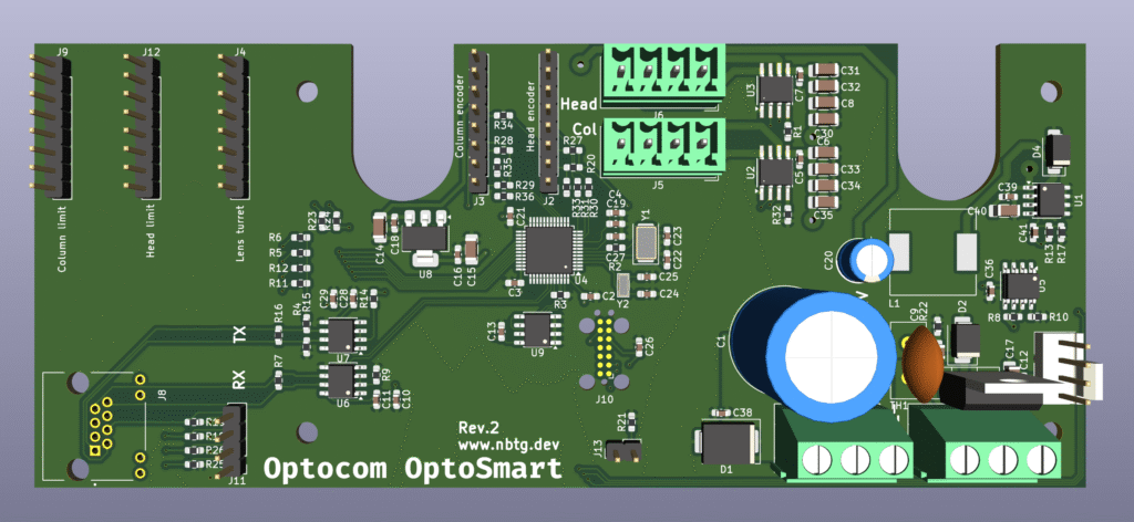
This 2-layer PCB controls and monitors both the head and column motors and encoders as well as any switches present (limits and lens turret), but also provides switching functionality for the lamp inside the enlarger head. I designed this to be paired with a 24VDC power supply, as halogen lamps can run on DC without issues. I have a 400W Mean-Well unit ready for use here; the lamp takes about 250W so there should be plenty for both motors and everything else. The advantage of this approach is that I only need a single power supply for both the color head and the enlarger itself.
The big change compared to the original PCB is that everything is controlled here, by a STM32F103 MCU, instead of externally via the control box. Because the system switches 24VDC at around 300W, I decided to go the RS485 over plain old Cat5 for robustness of communication, giving me 4 twisted pairs to use. This meant I could use 2 transceivers, one for upstream and one for downstream, to ensure no messages will be lost on either side. I might use the 2 remaining pairs for interrupt logic, but I don’t think it’ll be necessary with a good communication protocol. The idea is to build an external control box which only sends and receives packets over a RS485-based communication system.
Design choices
The PCB has a 24V net backed by a big 1000uF buffer cap and protected with a TVS and inline fuse (in the cable), a derived 12V net for the encoders and a MOSFET driver from a XL1509 (U1) and a 3v3 net derived from the 12v net from a AMS1117-3.3 (U8) for the MCU and the other logic.
Both encoders are NPN open collector, so the A/B/Z lines are pulled up to 3v3 to easily interface with the STM32. The STM32 has dual hardware quadrature inputs for easy decoding.
The switches are all floating unless closed, then they’ll be pulled to ground. I pulled up the lines coming from them to create a nice high-low transition for the MCU to recognize when a switch has been closed.
The motors are controlled using DRV8871DDA H-bridges instead of the older L298 parts. These are EOL parts, but with good availability, and cheap in JLCPCB’s part system.
Switching the lamp is done by using a IRLZ44N MOSFET driven via a UCC27424. I will probably have to design a heatsink for the MOSFET itself. The lamp is inrush limited using a B57127P508M301 0.5ohm inrush limiting NTC, I’ll have to check for exposure repeatability but it shouldn’t add more than a few ms to the full illumination time. I added a fan header for a 24VDC fan, which can be controlled via PWM. I used a Delta FFB1224EHE 120mm fan here, as the original fan is a blower type AC fan.
Connector J13 is an interface for an external NTC, which I’ll add to the lamp housing to monitor temperatures there so I can modulate the fan instead of having it run full power all the time like in the original design.
The system communicates over 2 dirt-cheap SP3485 RS485 transceivers, part of JLC’s basic part catalog. I opted for 2 instead of 1 to have a full-duplex system. Not that I need that much bandwith, but since I have pins to burn, who cares? The other 2 pairs are brought out to a 2.54mm header, and tied to ground when not in use. They’ll have to be floating on the other end, though. I might just use a Pi in a 3d-printed box with a SPI OLED display with a red filter instead of building another embedded system.
Now I just have to wait for JLC to deliver my finished PCB’s. 5 PCB’s, of which 2 fully assembled, for just under 60 euros? What a steal. I took this opportunity as well to finally buy a semi-decent soldering station, since I’ll have to mount some THT parts myself, and do some rework since I already found a few design mistakes. The revision pictured here is Rev.2, which already has them patched.
Next up, the actual PCB, reworks and preliminary firmware design.
1 thought on “Optocom – part 2 – PCB design”